연구/산학
PKNU Research 1000
| Park Woon-Ik | Developed 'dual nanopatterning process' for the first time | |||
| 작성자 | 대외협력과 | 작성일 | 2023-09-08 |
| 조회수 | 791 | ||
| Park Woon-Ik | Developed 'dual nanopatterning process' for the first time | |||||
 |
대외협력과 |  |
2023-09-08 |  |
791 |
PKNU developed 'dual nanopatterning process' for the first time
- joint research with Busan national univ., Korea university, POSTECH, and KICET

△ Researchers at Pukyong National University. From the left, professor Park Woon-Ik, Dr. Park Tae-Wan, master candidate Kang Young-Lim, and Kang Eun-Bin in integrated bachelor and master's program.
Pukyong National University announced that professor Park Woon-Ik's (materials science and engineering major) research team was the first to develop an advanced concept and technology of dual nanopatterning process that forms a 20-nano ultra-fine pattern on an 8-inch wafer in the semiconductor process.
With the development of next-generation electronic devices, the development of nanopatterning processes to implement highly integrated semiconductor circuits is essential to produce various electronic devices. Photolithography is mainly used as the current representative nanopatterning process, but researchers have been developing new processes to replace it due to limitations in pattern resolution, expensive equipment, and complicated process steps.
'Nanotransfer printing', which exhibits high pattern resolution at a low cost, is considered one of the new alternative processes, but this has also been pointed out as a disadvantage in that the pattern resolution is largely dependent on the pattern size of the master mold.
To solve this problem, the research team applied a method that combined the self-assembly phenomenon of block copolymers containing silicon (Si) with the nanotransfer printing process and finally they succeeded in developing a dual nanopatterning process to form regularly aligned 20-nanometer silica (SiOx) structures on an 8-inch wafer.
Professor Park Woon-Ik said, "I expect that the dual nanopatterning process will greatly contribute to the development of next-generation semiconductor technology in the future because it can implement highly integrated patterns with more complex circuits at a cost that is one-tenth of that of existing patterning technologies."
This research was conducted through the basic research laboratory (BRL) and mid-career researcher program provided by the National research foundation of Korea (NRF) under the Ministry of science and ICT (MSIT), and the paper containing the research results, 'direct printing of ultrathin block copolymer film with nano-in-micro pattern structures' was published in the international academic journal <Advanced science> (IF: 17.5) dated on August, 21.
The research was jointly attended by professor Park Woon-Ik, Dr. Park Tae-Wan, master candidate Kang Young-Lim, and Kang Eun-Bin in integrated bachelor and master's program, professor Hwang Geon-Tae at Pukyong National University, professor Kim Gwang-Ho (director of NRF global frontier project), professor Kwon Se-Hun, professor Lee Jung-Woo and professor Lee Seoung-Ki from Busan national university, professor Nam San from Korea university, professor Choi Si-Young from the Pohang university of science and technology (POSTECH), and doctor Jung Hyun-Sung from Korea institute of ceramic engineering and technology (KICET).
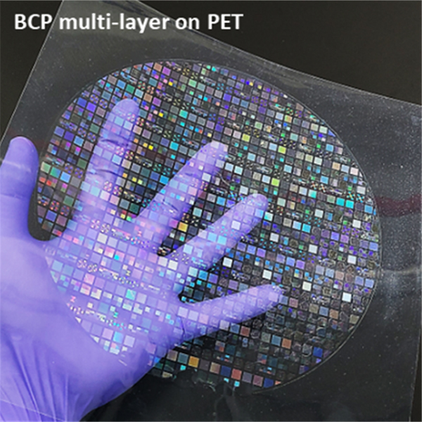
△ A 20-nano microcircuit structure formed on a flexible and transparent substrate through a dual nanopatterning process.