-
대학/대학원
-
연구/산학
-
대학생활
-
입학/취업
-
커뮤니티
-
대학소개
-
개교 80주년
커뮤니티
부경투데이
- 국립 부경대학교의 다양한 모습과 소식을 접하시면 부경대학교가 한번 더 가까워집니다.
| 차세대 에너지 변환소자 기술 이끈다(Leading next-generation energy conversion devices technology) | |||
| 작성자 | 대외협력과 | 작성일 | 2021-07-19 |
| 조회수 | 535 | ||
| 차세대 에너지 변환소자 기술 이끈다(Leading next-generation energy conversion devices technology) | |||||
 |
대외협력과 |  |
2021-07-19 |  |
535 |
‘플라스틱·유리에도 붙는다’ 차세대 2차원 열전박막 개발 ‘주목’
- 부경대 황재열 교수, 국제학술지 <ACS Energy Letters>에 발표
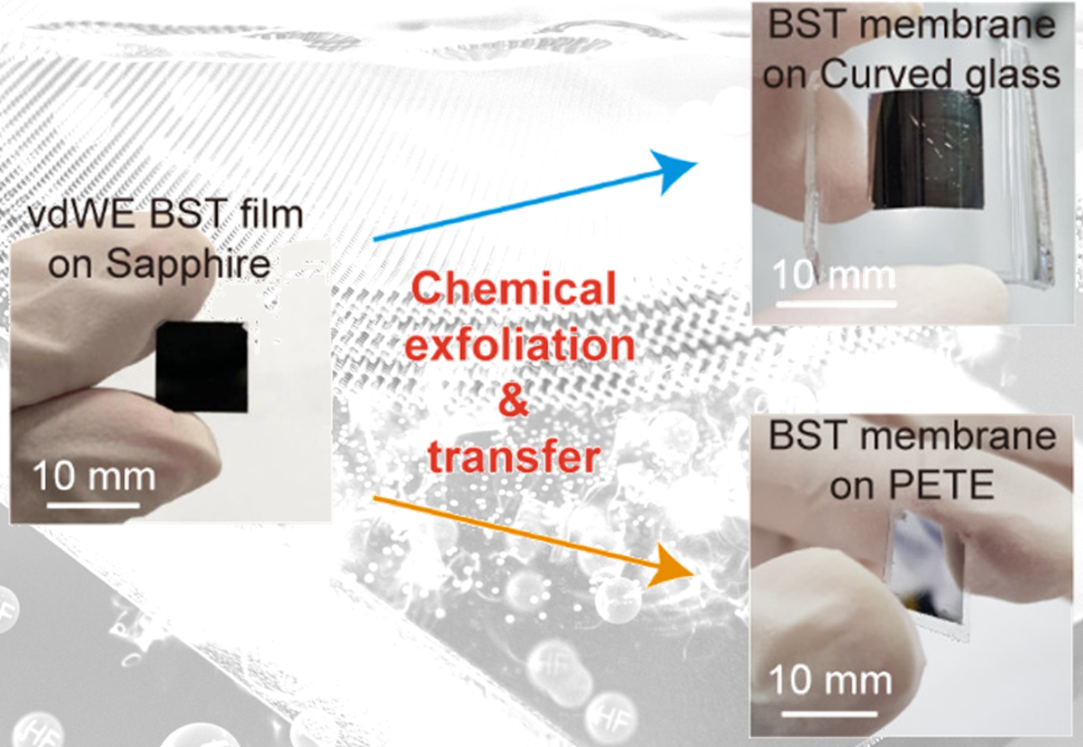
△ 고성능 2차원 열전박막을 분리해 평면과 곡면에 붙인 모습
차세대 에너지 변환소자로 주목받고 있는 고성능 2차원 열전박막을 반도체 기판(웨이퍼)은 물론, 플라스틱이나 유리에 전사(transfer)할 수 있는 기술이 개발됐다.
국립부경대학교 황재열 교수(물리학과)는 성균관대학교 김성웅 교수(에너지과학과)와 함께 고성능 2차원 열전박막을 기판에서 분리해 응용할 수 있는 기술을 개발해 과학기술 분야 세계적 학술지 <ACS 에너지 레터스(ACS Energy Letters, IF 23.101)>에 최근 발표했다.
열전박막이란 열을 전기에너지로 바꿔주는 열전소재로 만든 박막이다. 웨어러블기기, 사물인터넷, 스마트센서 등에 적용할 수 있는 차세대 소자로, 최근 2차원 구조 박막에서 우수한 물성들이 발견돼 관련 연구가 증가하고 있다.
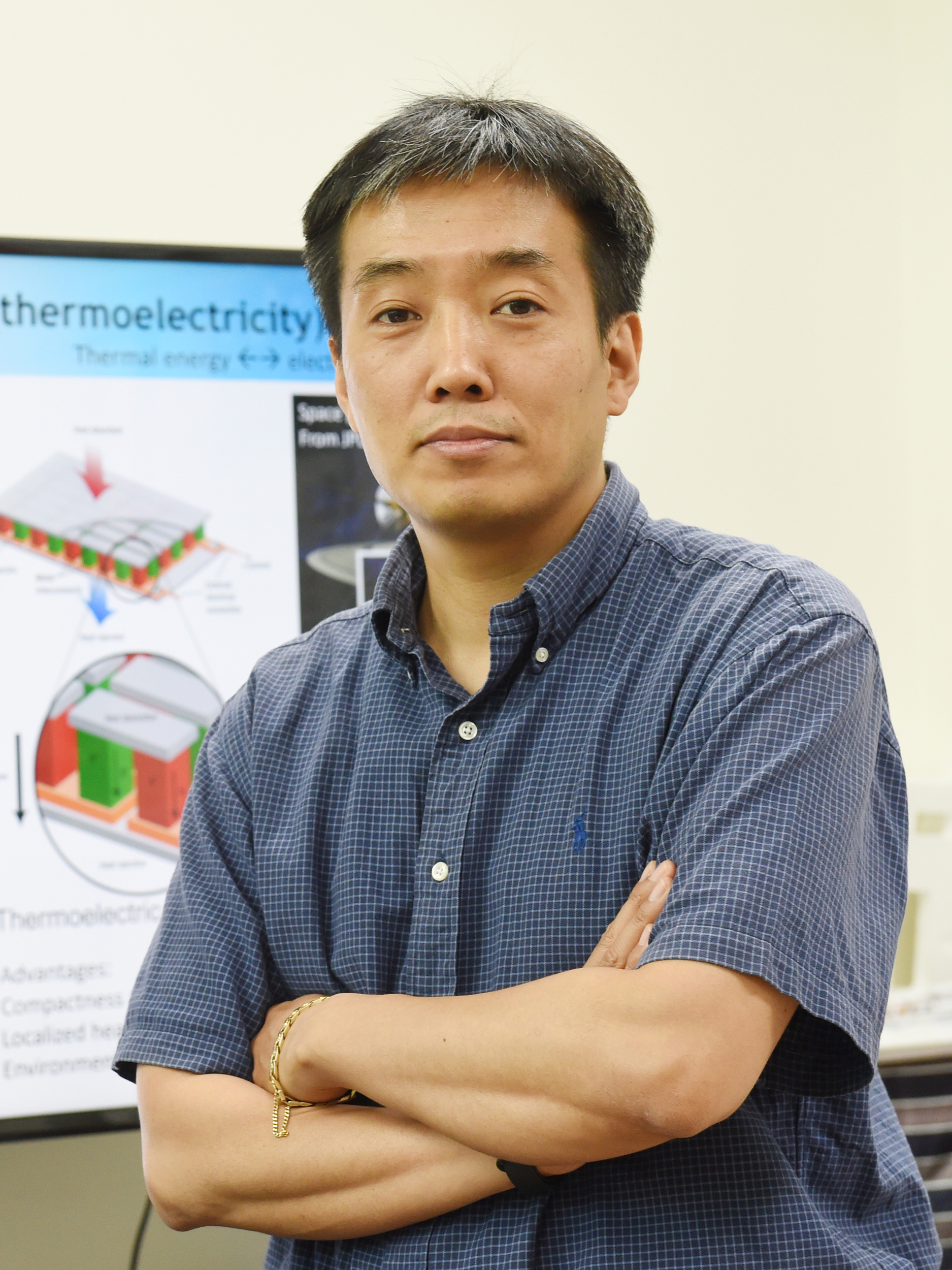
△ 황재열 교수 사진 ⓒ사진 이성재(대외홍보팀)
황 교수 연구팀은 에피탁시(epitaxy) 공정(기판 위에 고순도의 단결정 박막을 성장시키는 공정)으로 박막을 성장(형성)시킨 뒤, 이 박막을 기판에서 손상 없이 분리해 평면은 물론 곡면에 붙여 우수한 열전에너지 변환효율을 달성할 수 있는 기술을 개발해냈다.
연구팀은 텔루륨 단원자층을 사파이어 기판 표면에 형성한 후 2차원 열전박막(BST)으로 성장시켰다. 이때 원자 간의 상호작용인 반데르발스 힘을 이용한 에피탁시 공정으로 기판과 박막이 약하게 결합하도록 하고, 용매를 이용해 이 결합을 선택적으로 제거해 결정구조를 유지하면서도 물성손실을 최소화해 분리하는 데 성공했다.
황 교수는 “이번 연구로 지금까지 제한적인 기판에서만 성장시킬 수 있었던 고성능 2차원 열전박막을 기판은 물론, 플라스틱이나 유리 등 다양한 형태의 물질에 전사해 활용할 수 있게 돼 신개념의 소자 개발 및 2차원 박막의 새로운 응용 가능성을 제시했다는 점에서 의의가 있다.”라고 말했다.
이어 “이번 연구는 반도체와 전자 분야에 널리 사용되는 사파이어 기판의 표면물성에 기반을 두고 있어 다양한 응용기술을 적용할 수 있고, 웨어러블 디바이스 등에 활용할 수 있는 고성능 박막형 에너지소자 등을 개발할 수 있을 것으로 기대한다.”라고 밝혔다. <부경투데이>
'Academic interest' in the development of a high-performance 2D thermoelectric thin-film that 'sticks to plastics and glass'
- Prof. Hwang Jae-Yeol at PKNU, published in the international academic journal <ACS Energy Letters>
A technology that can transfer a high-performance two-dimensional thermoelectric Membrane to semiconductor substrates (wafer), as well as plastic or glass, which is attracting attention as a next-generation energy conversion device, has been developed.
Professor Hwang Jae-Yeol (Dept. of Physics) at Pukyong National University, together with Professor Kim Sung-Wng (Department of Energy Science) at SungKyunKwan University, developed a technology that can separate and apply a high-performance two-dimensional thermoelectric thin film from a substrate, and recently published their findings in the world-renowned scientific journal (ACS Energy Letters, IF 23.101)>.
A Thermoelectric Membrane is a thin film made of thermoelectric material that converts heat into electrical energy. It is a next-generation device that can be applied to wearable devices, the Internet of Things, and smart sensors. Research related to this has been increasing since the recent discovery of excellent properties in 2D thin films.
Professor Hwang's research team has developed a technology that can achieve exceptional thermoelectric energy conversion efficiency by growing (forming) a thin film through an epitaxial process (vdWE: spontaneous van der Waals epitaxy), then separating the epitaxial thin-film from the growth substrate without damage and transferring it onto a curved surface or a flat surface.
The research team succeeded in transforming a pseudo-morphic Te (tellurium) monolayer on the surface of a sapphire substrate and grown as a BST membrane. At the same time, they made the substrate and the film weakly bond through an epitaxy process using the van der Waals force, an interaction between atoms, and selectively removed this bond using a solvent to maintain the crystal structure while minimizing the loss of physical properties.
Professor Hwang said, "Through this research, high-performance two-dimensional thermoelectric thin-films, which could only be grown on limited substrates, can be transferred and utilized not only on the substrates but also on various types of materials such as plastics and glass. In this regard, this study suggested the development of a new concept device and the possibility of the new application of the 2D thin-film."
"As this research is based on the surface properties of sapphire substrates widely used in semiconductor and electronic fields, I am expecting that various applications of this technology can be applied in the future, and high-performance thin-film energy devices that can be used in wearable devices can be developed," he added. <Pukyong Today>